Product Information
Home > Product Information > Target · Vapor deposition material · Vapor deposition source > Sputtering target
Sputtering target
We will provide semiconductor, FPD, optical devices, recording media, the sputtering target of various kinds for the thin film material of the hard coating and energy-related, and the like.
Making full use of extensive network of domestic and overseas, we will propose the best products to our customers' needs from research and development for the prototype to mass production.
Products List
Handling target list
| metal (Metal) |
Al · C · Cr · Cu · Ge · Co · Au · Hf · In · Fe · Pd · Mg · Mo · Ni · Nb · Pt |
|---|---|
| Se · Si (Multi & Mono) · Ag · Ta · Ti · Sn · W · Zn · Zr · V · etc. | |
| Oxide (Oxide) |
Al2O3 · CeO2 · Cr2O3 · CuO · Ga2O3 · GeO2 · In2O3 · La2O3 |
| MgO · MnO2 · Nb2O3 · SiO2 · Ta2O5 · TiO2 · WO3 · ZnO · etc | |
| Transparent conductive film (TCO) |
ITO (In2O3: SnO2) · AZO (ZnO: Al2O3) |
| GZO (ZnO: Ga2O3) · IGZO (In: Ga: ZnO) | |
| Others (Rest of Targets) |
Carbides (carbide) · Florides (fluoride) · Nitraides (nitride) |
| Alloy (alloy) · AgAlloy · AlAlloy · CoAlloy · CrAlloy · NiAlloy · TiAlloy · etc |
* Material other than the above are also available. Please specify the specification of your choice (material, purity, size, etc.).
- Bonding processing
Make the best bonding to various target material. Also we will correspond to re-bonding from the collection of used targets.
- Backing plate production
We manufacture various kinds of backing plate by cultivated precision processing technology in the semiconductor and LCD manufacturing equipment vacuum parts manufacturing.
- Indium ingot sales
Making full use of extensive network of domestic and international, will be sold a high-quality low-cost bonding for indium ingot. In addition also responsible for the recovery and purification.
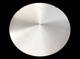
Si target

We have abundant silicon material handling through Si test wafer business and Si recycling business for semiconductor industry and solar cell industry.
Purity of the single and multi-crystalline silicon material in response to customer requests, resistance value, we offer you is processed into a size and shape.
Si target
ITO target demand rapidly as the transparent conductive film has been expanding. But indium is the main component is a rare element, the soaring prices and supply anxiety is a problem.
For this reason the ZnO-based as the ITO alternative material that is in urgent need development (GZO, AZO) We propose a target.
GZO, AZO target (for the transparent conductive film)
It is possible to use vapor deposition to make materials suitable for deposition. In addition, certain degassed products suppress gas emission from vapor deposition materials to a low level, and this adversely affects the strength and durability of thin films.
| Use | Transparent conductive film, TFT-LCD, OLED, thin film solar |
|---|---|
| purity | 3N |
| density | 5.5g / cm3 |
| Maximum length | 550 mm |
| The greatest width | 300 mm |
| Maximum thickness | 12 or 20mm |
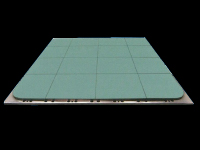
Cr target
| Use | TFT-LCD, OLED, PDP, color filter, photomask, hard coating |
|---|---|
| purity | 3N, 3N5, 4N, 4N5 |
| Maximum length | 2500 mm |
| The greatest width | 1500 mm |
| Maximum thickness | 50 mm |
| accuracy | 0.5 mm |
| Surface roughness | Grinded Ra 1.6um |
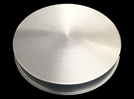
AI target
| Use | Solar cells, organic EL · semiconductors and recording media |
|---|---|
| purity | Can correspond up to 5N5 |
* U, there is also the handling of controlled material to Th amount of impurities <1ppb.
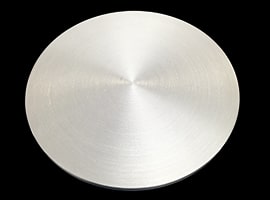
Ti target
| Use | Semiconductor and optical glass-hard film other |
|---|---|
| purity | Can correspond up to 5N5 |
