Product Information
Home > Product Information > Wafer glass service > Patterned wafers
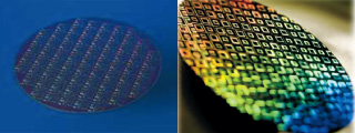
Patterned wafer
- Line & Space, Contact Hole
- I-Line, KrF, ArF, ArF immersion
- CMP TEST (Cu, W, STI, ILD etc.) - 754, 854, 454Mask, etc., Various Novati Mask compatible types
- Plasma Damage TEG
* Corresponds to the minimum line width of 32 nm and is available from mask production.
* Required meeting. Please contact us for more information.
Pattern Wafer Products
Cu CMP Evaluation wafers
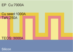
| Size | 300 mm |
|---|---|
| Construction | Anneal / Cu EP 7KA Fill / Cu seed 1K / TaN 250A / Etch 3K (100nm Trench) / TEOS 3K / Si |
W CMP Evaluation wafers
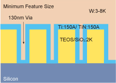
| Size | 300 mm |
|---|---|
| Construction | W 3K ~ 8K Fill / Ti: 150A / TiN: 150A Etch 3K ~ 8K / (130nm Via) PE-TEOS 2K / Si |
STI CMP Evaluation wafers
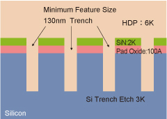
| Size | 300 mm |
|---|---|
| Construction | HDP 6K Fill / Si etch 3.5K (130nm Trench) SiN 2K / Pad Ox 100A / Si |
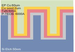
TSV(Through Silicon Via) Wafer
| Size | 300 mm |
|---|---|
| Construction |
EP Cu 60um Fill / Cu seed 2um / TaN 600A / PE-TEOS 6K / Si Via etch 50um / Si |
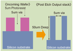
Deep Si Etch (50um) via Wafer
| Size | 300 mm |
|---|---|
| Construction | Si Via etch 50um / Si |
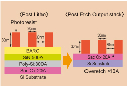
Double Patterning Wafer
| Size | 300 mm |
|---|---|
| Construction | Etch (30nm Trench) 300A Poly Si +/- 5% 20A Sac Ox / S |
* Specifications other than the above are also available. Please specify the specification of your choice.